Traditionally, laser scanning galvanometers paired with lasers have been primarily used in marking and rapid prototyping. These systems can provide high-quality beams, but the laser power is typically limited to the range of hundreds of watts. Nowadays, with the advent of high-brightness lasers such as fiber lasers, disk lasers, and even some high-power diode lasers with lower brightness, the application range of scanning galvanometers has expanded to the kilowatt level. Scanning devices must be capable of handling high power applications without compromising precision and speed, which presents a significant challenge for galvanometer manufacturers.
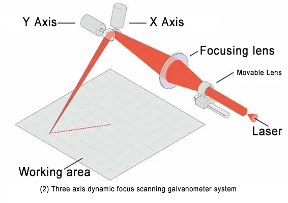
A basic x-y scanning device appears simple: two mirrors driven by motors can reflect the incident laser beam to any point within a specific area (working area). A set of flat-field (f-θ) lenses ensures that the focus remains within the plane of the working area (two-axis system, as shown in Figure 1). For basic Nd:YAG lasers, the typical working range is from 40×40 square millimeters (f-θ = 100 mm) to 180×180 square millimeters (f-θ = 254 mm). For advanced harmonic lasers and diode lasers, the working range is from 40×40 square millimeters (f-θ = 100 mm) to 120×120 square millimeters (f-θ = 163 mm), depending on the focal length of the flat-field lens. Clearly, the larger the required working range, the longer the working distance. If a combination of focusing lenses and movable lenses is used in the laser path before the scanning galvanometer instead of flat-field lenses, the working range and working distance can be further increased (three-axis system, as shown in Figure 2). This setup can achieve a working range of 1200×1200 square millimeters and a working distance of 1500 millimeters.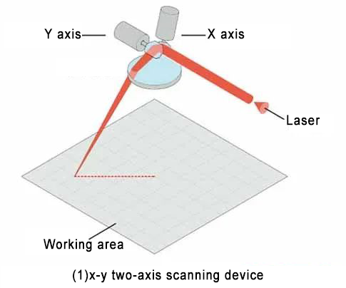
In many applications, high positioning speed is required. For example, when the focal length of the f-θ lens is 163 mm, the scanning speed within a 120×120 mm² working area can reach 10 m/s. Simple geometric calculations show that even a small angular deviation of the galvanometer mirror can cause significant misalignment of the laser spot on the working plane. Therefore, high-level positioning accuracy is essential for the galvanometer drive, mirror, and mirror mount. Additionally, the galvanometer motor and driver electronics generate heat, causing thermal drift and resulting in positioning errors. Thermal gain drift characteristic values are <30 rad/K, and gain drift characteristic values are <50 ppm/K (per axis). Therefore, if high precision and long-term stability are required, one solution is to opt for scanning galvanometers with water cooling. A representative example is the Superscan-II-LD, which can achieve long-term stability of <200 rad over 24 hours (without active cooling, <300 rad). Moreover, systems with integrated automatic calibration functions can reduce gain drift to 20 rad/K and position drift to 5 ppm/K, achieving long-term stability of <20 rad over 8 hours.
In marking applications, the types of mirrors used in scanning galvanometers include quartz substrate materials with thicknesses ranging from 2.0 to 7.0 mm, depending on the mirror size and angular acceleration. Electrolytic coatings provide sufficient reflectivity (>98.0%) within the corresponding wavelength range (e.g., for high-power semiconductor lasers and deflection ranges exceeding ±12° at 780 nm and 980 nm). These mirrors can typically withstand power densities of up to 500 W/cm², which is more than sufficient for traditional marking applications. However, introducing scanning heads into other applications brings new challenges, such as polymer welding. These applications require precise control of the workpiece temperature, usually measured non-contact using pyrometers. For this technology, the thermal radiation signal from the workpiece must return to the sensor along the laser path, for example, reflected back through the galvanometer mirror. The typical wavelength range for high-temperature measurement is 1.7 to 2.2 μm. Since dielectric layers are penetrable by laser radiation within this wavelength range, an aluminum coating on the back of the quartz substrate can solve the problem. It should be noted that if the wavelength range is to be extended, the scanning optical system needs to be adjusted accordingly.
Other new high-power applications, such as laser remote welding, remote cutting, or scanning heat treatment, require power levels ranging from hundreds of watts to even several kilowatts, posing new challenges for galvanometer scanning heads. Even if the reflectivity of dielectric mirrors is very high (especially with an aluminum coating), a portion of the light (<2%) may still be transmitted and absorbed by the mirror substrate or surrounding components. For low-power lasers, this is manageable. However, high-power lasers can generate significant heat inside the device, leading to noticeable thermal drift and unacceptable long-term stability fluctuations. Therefore, water cooling for the scanning device is essential but usually insufficient. This is because it cannot prevent the thermal load on the quartz mirror and its resulting effects, such as deformation or softening of the adhesive layer or galvanometer drive failure due to rotor and bearing heating. Thus, new mirror technologies are indispensable.
One major drawback of quartz is its low thermal conductivity, resulting in poor cooling performance. Silicon-based materials, such as silicon or silicon carbide, offer higher thermal conductivity. Due to the higher strength of silicon carbide materials, their thickness can be reduced, and despite their higher density, the overall mass can be lightened. If opaque substrates like Si or SiC are used, a broadband reflective aluminum layer can be directly coated on the dielectric layer between the dielectric film and the silicon substrate. Careful modeling calculations of the mechanical design of the mirror substrate can optimize stability, weight, thermal conductivity, and rotational inertia.
For system design, including servo circuit boards, galvanometer motors, and mirrors, several parameters need to be particularly precise:
Mirror weight;
Mirror torque;
Mirror deformation (mechanical spring);
Deformation of the connection between the mirror and the drive motor;
Response frequency of the mirror and drive motor system.
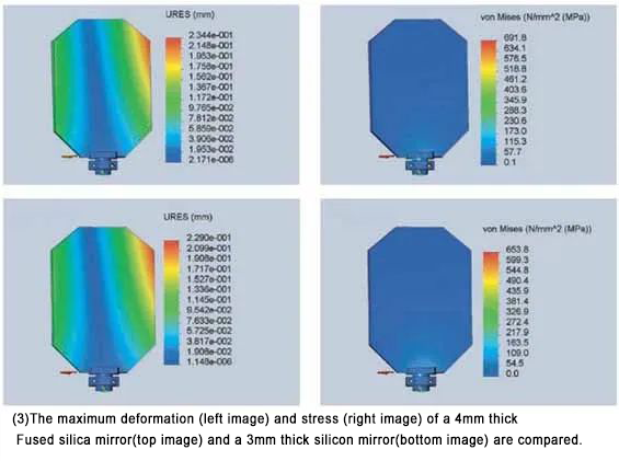
Using silicon as the substrate can reduce the mirror thickness (weight) while maintaining the same deformation, stress, and thickness as a quartz substrate mirror (see Figure 3). However, due to the weight, stress, and deformation of the mirror system, these improvements are insufficient to meet market demands for higher scanning speeds and higher power densities, especially for kilowatt-level high-brightness lasers. These applications require new materials and designs to further reduce substrate thermal stress. Ceramic materials with higher stiffness than silicon or quartz, such as silicon carbide, are better choices. However, designing SiC mirrors is far more challenging than standard silicon or quartz mirrors, necessitating a complete overhaul of the mirror design approach. Finite element analysis and Monte Carlo analysis are very useful tools in this design. The main design goal is to reduce high-frequency and ultra-low-frequency components as well as weight and moment of inertia. To this end, we designed a completely new back structure for the mirror, as shown in the left image of Figure 4. This mirror has much higher stiffness than silicon mirrors, and due to the lighter substrate and different Young’s modulus, stress is easier to manage. Calculations clearly show that the maximum deformation and stress of the mirror have been improved.
 This approach achieves high precision and excellent mechanical performance (minimizing resonance response effects). The high thermal conductivity of the mirror material allows for rapid temperature distribution balance, even when absorbing significant laser energy under high-power lasers. The reinforcing ribs on the back of the mirror provide a larger surface area for heat transfer to the surrounding atmosphere and more efficient radiative cooling. The mirror has a very uniform temperature distribution and a relatively gentle temperature gradient.
Unfortunately, SiC is very difficult to work with. Firstly, due to its hardness, it is extremely challenging to process. Secondly, unlike silicon or quartz substrate coating processes, it is impossible to coat the back of the substrate. The back coating helps counteract the mechanical stress generated by the coating itself (i.e., different coefficients of thermal expansion). The result of this stress is usually a concave reflective surface, causing undesirable defocusing effects. Thirdly, the required material quality and quantity are very difficult to obtain, and long delivery times make logistics risky. This issue can lead to prolonged R&D times and still result in long delivery times. Therefore, the search for alternative materials continues.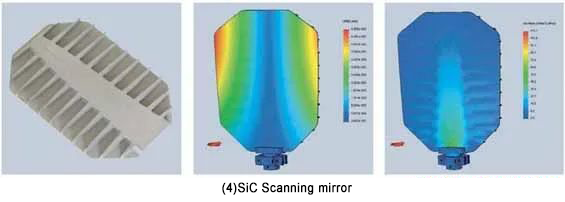
One alternative material is beryllium, which can be used as a substrate material. This material is lightweight and offers high thermal conductivity. Beryllium is readily available, with reasonable delivery times, and is easier to process than silicon carbide due to its lower hardness. However, this material also has drawbacks. Firstly, it is highly toxic. Since this material is already used in many products, such as satellites or military flight systems, this issue can be addressed through mature commercial processing techniques. To avoid skin contact with beryllium, the entire surface is coated with nickel. Due to the large grain size of beryllium, it cannot be polished to a flatness of less than λ/4 at 630 nm, so nickel is used for polishing and coating. Another advantage of this process is that it provides high surface quality.
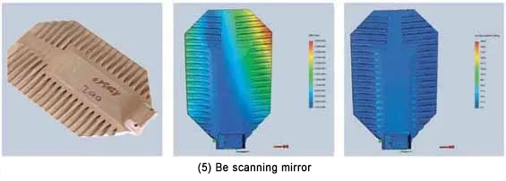
Additionally, optimized parameters based on model calculations ensure the best design. Due to the lower density and relatively high Young’s modulus, the design of beryllium models is simpler compared to silicon carbide models. Another advantage of this material is its absorption capacity. Comparing beryllium and silicon carbide mirrors, the beryllium model has two fewer critical frequencies than the silicon carbide model. This provides simpler automatic control capabilities for the servo circuit board and galvanometer motor. As a result, the beryllium mirror is 35% lighter and has 35% less inertia than the silicon carbide mirror. The mirror design, maximum deformation, and maximum stress are shown in Figure 5.
Furthermore, significant progress has been made in integrating the mirror mount and mirror model, meaning no adhesive or clamping is required. The mirror and holder are machined as a single piece and directly fixed to the galvanometer motor shaft. This results in reduced mass, improved stiffness, and increased thermal conductivity. Additionally, the system eliminates the risk of overheating and damage to the adhesive layer. This design significantly improves the mirror’s specifications. For example, compared to standard silicon carbide mirrors installed in typical scanning heads, the final speed can be increased by 30%, saving 20% of the time. Users can benefit from increased speed or higher dynamic performance with larger aperture scanning heads. This improvement allows for a smaller focal plane diameter and working distance within the same field of view size or an increased field of view size and working distance with the same focal length size.
Beryllium material meets market demands in many aspects, such as shorter new product development cycles, and the mirror model, mirror size, and application requirements can be precisely matched. To achieve the best speed results, mirrors should be designed to reflect the required beam angle and beam size.
With the emergence of new applications, scanning head manufacturers face new requirements, such as metrology integration (pyrometers, cameras) to meet the needs of applications like welding and polymer contour welding. However, as mentioned above, high power and high brightness lasers bring many other requirements to high-precision scanning heads, but they also open up new markets beyond traditional marking applications. Many applications now use new technologies and are still privately patented.
Nevertheless, even traditional laser processing, such as welding, cutting, or surface treatment, now requires scanning galvanometers. For example, high-brightness lasers can cut thin metal sheets at high speeds, exceeding the limits of traditional positioning systems due to weight and inertia. Therefore, part positioning has been replaced by “inertia-free” laser beam positioning. This processing method is known as “remote cutting.”
For welding applications, the well-known “remote welding” process can be modified using a combination of robot positioning and high-speed scanning heads (“3D scanning welding”). It has been proven that this method can almost reduce laser non-working time to zero (depending on the position and structure of the weld seam). When the robot performs smooth movements along the contour, the “jumping” deviation from one weld seam to the next can be controlled by the high-precision, high-speed scanning of the scanning head. In this “scanning welding” application, the key factor is the software, which combines the position and speed of the robot with the beam positioning controlled by the scanning head.
Due to the emergence of highly efficient laser sources in the 1-micron wavelength range (such as high-power semiconductor lasers), laser hardening and laser cladding have now become standard processes in the machine tool market. Localized heat concentration can prevent part deformation and damage, significantly reducing rework. However, the challenge of laser surface hardening is achieving the ideal temperature distribution on the part surface. This can be achieved through special optical systems that “shape” the laser intensity profile, but this method is very complex and rigid. A more flexible and reasonable solution is to combine rapid laser beam scanning with rapid laser output power control. This type of device, working in conjunction with a pyrometer, can achieve almost any type of temperature distribution and uniform temperature control.
Since the mid-1990s, laser polymer welding has become a standard tool for automotive parts, mechanical devices, electronic components, and consumer products. It initially started with contour welding, where the laser moves slowly along the weld seam. However, it has gradually evolved into various methods, such as seam welding or synchronous welding, and has developed into today’s advanced technology. The advantage of synchronous processing (such as softening the entire welding structure) is the welding path, meaning the relative movement of the parts to be welded can be used as a process control parameter. Unfortunately, synchronous laser welding requires the geometric shape of the laser heat source to match the geometric shape of the weld seam, making the technology very complex, expensive, and inflexible. A smart solution is “semi-synchronous” welding, where the laser beam repeatedly moves along the entire weld seam structure, heating the entire weld seam to above the softening point, achieving synchronous welding and weld path control. Since the welding profile can be easily changed through software, this method is very flexible. Of course, this method is limited to planar structures (or at least approximately planar), with a scanning area size within 400×400 mm, and the laser power can be matched; additionally, the required speed and laser power can be proportional to the weld seam length. Besides flexibility, this device also allows for online process control due to the use of scanning heads and the aforementioned optical systems.
By improving precision, speed, and laser power, scanning galvanometers have become a very important tool in laser processing. Their market has expanded from traditional marking and rapid prototyping to laser material processing in various fields, including cutting, welding, surface treatment, polymer welding, and other applications. Bena Optics’ scanning galvanometer technology, combined with innovative mechatronic design concepts, especially new materials and intelligent solutions for mirror technology, has adapted to new market demands. High-brightness laser sources have opened up a bright future for scanning galvanometers.