1. Principles of Geometric Optics
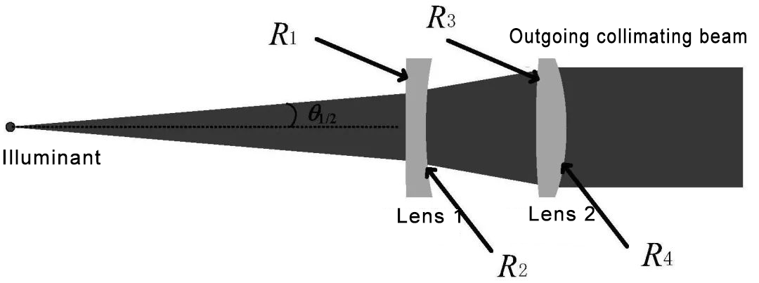
Laser collimating Lens primarily rely on the principles of geometric optics, specifically the refraction and reflection laws governing lenses or Lens. When a laser beam enters a collimating mirror system, for lens-based systems, it utilizes a combination of lenses with different curvatures.

For example, convex lenses converge light rays, while concave lenses diverge them. By carefully designing the focal lengths and spacing of convex and concave lenses, a laser beam with a certain divergence angle can be transformed into a parallel beam after passing through the lens assembly.
In mirror-based systems, parabolic Lens are commonly used. According to the optical properties of parabola, light rays emanating from the focal point of a parabolic mirror will reflect and exit parallel to the symmetrical axis. Therefore, placing the laser source at the focal point of a parabolic mirror can produce a collimated laser beam.
2. Principles of Physical Optics (Considering Laser Characteristics)
Lasers possess characteristics such as coherence, monochromaticity, and directionality. During the collimation process, the wavefront properties of the laser must be considered. The design of the collimating mirror should ensure minimal wavefront distortion.
The interference principle of light waves can be used to test and optimize the performance of collimating Lens. For instance, an interferometer can measure the difference between the laser wavefront after passing through the collimating mirror and an ideal plane wave, thereby guiding improvements in the design and manufacturing process of the collimating mirror.
Functions of Laser Collimating Lens
1. Beam Collimation
The primary function is to transform a laser beam with a certain divergence angle into a parallel beam. This allows the laser to maintain a small spot size and high energy density over long distances.
For example, in long-distance laser communication or laser ranging applications, a collimated laser beam can reduce energy loss during propagation, enhancing the transmission distance and accuracy of the signal.
2. Beam Shaping
Besides collimation, collimating Lens can also adjust the shape of the laser beam. For instance, transforming a circular laser spot into a square or elliptical shape to meet the requirements of different application scenarios.
In laser processing, different spot shapes can result in varying processing effects. By using collimating Lens for beam shaping, the processing technique can be optimized.
3. Energy Control
Precisely controlling the energy distribution of the laser beam. Through the design and optimization of collimating Lens, the laser energy can be uniformly distributed or distributed according to a specific pattern in the collimated beam.
In applications requiring high uniformity of laser energy, such as laser annealing or laser thin-film deposition in semiconductor manufacturing, this energy control function is crucial.
Applications in Semiconductor Metrology
1. Lithography Alignment
In semiconductor lithography, it is essential to accurately transfer the patterns on the photomask to the silicon wafer. Laser collimating Lens can provide precise alignment beams for lithography equipment.
For example, by emitting a collimated laser beam to determine the relative position of the photomask and the silicon wafer, ensuring high-precision pattern transfer. Given that lithography processes require nanometer-level precision, the high-precision collimated beams provided by laser collimating Lens are critical for ensuring lithography quality.
2. Wafer Flatness Measurement
Used for measuring the flatness of wafer surfaces. During measurement, a collimated laser beam is directed at the wafer surface at a certain angle, and the flatness is analyzed by measuring the angle and intensity changes of the reflected light.
Since laser collimating Lens can provide stable and directionally precise laser beams, this measurement method offers high accuracy and reliability, helping to select wafers that meet quality standards and ensuring the performance and yield of semiconductor chips.
3. Chip Defect Detection
In chip defect detection systems, laser collimating Lens can provide the detection light source. A collimated laser beam can be focused on a small area of the chip surface, and defects such as scratches or holes can be detected by analyzing the characteristics of the reflected or scattered light.
This high-precision detection technology relies on the high-quality laser beams provided by collimating Lens, enabling early detection and localization of chip defects, reducing the production of non-conforming products, and improving the production efficiency and product quality in semiconductor manufacturing.